 sales@aoelectronics.com
 +86 755 2821 9272


Manufacturers
- Abracon
- Adam Tech
- Aerospace, Defense & Marine
- Agastat
- AIC
- AKM Semiconductor
- Alcoswitch
- Allegro
- Alps Electric
- Altera
- AMI Semiconductor
- AMP
- ams
- Analog Devices (ADI)
- Aptina Imaging
- Atmel
- Avago / Broadcom
- AVX
- Axicom
- Bccomponents
- Beyschlag
- BI Technologies
- Bourns Inc.
- Bowei Integrated Circuits
- Bridgelux
- Buchanan
- California Micro Devices
- Catalyst Semiconductor
- CGS
- Cirrus Logic
- Citizen Electronics
- CML Microcircuits
- Coiltronics
- Cooper Bussmann
- Corcom
- Core Logic
- Cree
- CSR PLC
- CTS
- Cypress Semiconductor
- Dale
- Data Image
- Deutsch
- Diodes Incorporated
- DOMINANT Opto Technologies
- E-T-A
- Eaton
- ECS
- Edison Opto
- Elcon
- EPCOS
- Epistar
- Epson
- Everlight Electronics
- Exar
- Fairchild Semiconductor
- FCI
- Freescale Semiconductor
- Fremont Micro Devices (FMD)
- Fujitsu Semiconductor
- Fulltech Electric
- General Semiconductor
- Harvatek
- Holsworthy
- Hsuan Mao Technology
- IDT
- Infineon Technologies
- Innolux
- International Rectifier (IR)
- Intersil
- IRC
- ISSI
- IXYS-IC
- Jing Cheng Electronical
- JL World
- Johanson Dielectrics
- Johanson Technology
- JRC / NJR
- JST
- KEC
- Kilovac
- Kingbright
- Kyocera Industrial Ceramics
- LEDiL
- Linear Technology / ADI
- Lite-On Technology
- Littelfuse
- Lumex
- Lumileds
- Luminary Micro
- Luminus Devices
- Macronix
- Maojwei / ZJPT
- Maxim Integrated
- MCC
- Mean Well Enterprises
- Microchip Technology
- Micron
- Microsemi
- Mini-Circuits
- Molex
- Murata Manufacturing
- Murata Power Solutions
- MWT
- National Semiconductor
- Nichicon
- Nippon Chemi-Con
- NJR / JRC
- NVE
- NXP Semiconductors
- OEG
- Omnivision
- ON Semiconductor
- Optek Technology
- Optrex
- OSRAM Opto Semiconductors
- OTAX
- Panasonic
- Peregrine(pSemi)
- Potter & Brumfield
- Power Integrations
- PowerStor
- Preci-Dip
- Prewell
- Products Unlimited
- Pulse Electronics
- PulseCore Semiconductor
- Qorvo
- Raychem
- Renesas Electronics
- RFMD
- Richtek Technology
- ROHM Semiconductor
- Rubycon
- Samsung Electro-Mechanics
- Samsung Semiconductor
- Schaffner
- Schrack
- Seiko Instruments, Inc. (SII)
- Semtech
- Sensata
- Seoul Semiconductor
- Sfernice
- Sharp Display
- Sharp Microelectronics
- Silicon Labs
- Siliconix
- Skyworks Solutions
- SoniCrest / JL World
- Spansion
- Sprague
- Stanley Electric
- STMicroelectronics
- Sunny Electronics
- Susumu (SSM)
- Taimag
- Taiyo Yuden
- TDK
- TDK-Lambda
- TE Connectivity
- Teccor
- Texas Instruments (TI)
- Thin Film
- Tianma Micro-electronics
- TOCOS
- TOKO
- Toshiba Electronic Components
- TT Electronics
- Tusonix
- TXC
- Tyntek
- Vishay
- Vishay Precision Group
- Vitramon
- Walsin Technology
- Weidmuller
- Welwyn
- Wickmann
- Winbond
- Xilinx
- Yageo
- Zetex Semiconductors
- ZJPT / Maojwei
News
ROHM’s New MOSFETs: Contributing to Higher Efficiency and Safer Operation with an Original Insulation Structure
2022-12-19 | Return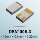
In recent years, the increasing sophistication and power requirements of compact devices have resulted in larger batteries that reduce the space available for mounting components. At the same time, there is a limit to the size of the battery, so to ensure more efficient use of battery power the power loss of mounted components must be minimized.
To meet this need, the development of MOSFETs in wafer-level chip-size packages (WLCSP) that contribute to greater miniaturization while maintaining the necessary characteristics is becoming mainstream in the industry. ROHM leverages its strengths as an IC manufacturer to significantly reduce wiring resistance (which has increased with conventional discrete processes). The result is a compact power MOSFET that delivers low power loss.
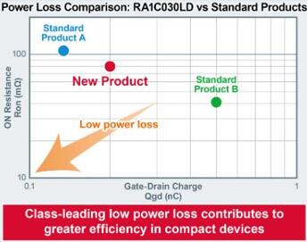
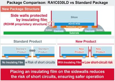
The RA1C030LD is offered in the DSN1006-3 wafer-level, chip-size package (1.0mm × 0.6mm) that takes advantage of ROHM’s proprietary IC process to achieve low power dissipation together with greater miniaturization. In terms of the figure of merit that expresses the relationship between conduction and switching losses (ON-resistance × Qgd), an industry-leading value has been achieved that is 20% lower than standard package products in the same package (1.0mm × 0.6mm or smaller), contributing to a significantly smaller board area along with higher efficiency in a variety of compact devices. At the same time, ROHM’s unique package structure provides insulated protection for the side walls (unlike standard products in the same package with no protection). This reduces the risk of shorts due to contact between components in compact devices that must resort to high density mounting due to space constraints, contributing to safer operation.
Going forward, ROHM will continue to develop products with even lower ON resistance in smaller package sizes that contribute to solving social issues such as environmental protection by improving efficiency in a variety of compact devices.
Specifications
Part No. |
Data |
Drain- Source Voltage |
Drain Current 4.5V |
ON Resistance 4.5V [mΩ] |
Gate- Drain Charge 4.5V [nC] |
Package |
20.0 |
3.0 |
80.0 |
0.2 |
DSN1006-3 |
Application Examples
◇ Hearables (i.e. wireless earbuds)
◇ Wearables such as smart watches, smart glasses, and action cameras
◇ Smartphones
Also suitable for switching in a wide range of thin, compact devices.
Online Sales Information
Sales Launch Date: December 2022
Terminology
● Nch MOSFET
A type of MOSFET that conducts when a positive voltage is applied to the Gate relative to the Source.
The smaller Drain and Source ON resistance vs Pch MOSFETs results in lower steady state loss.
● Wafer-Level Chip-Size Package (WLCSP)
An ultra-compact package in which the terminals and wiring are formed on wafers before they are separated into individual pieces. Unlike general packages where the wafers are individually cut before the terminals and other components are formed then encapsulated with resin mold, the package can be made the same size as the semiconductor chip itself, making it possible to further reduce package size.
● ON Resistance
The resistance value between the Drain and Source while the MOSFET is ON. The smaller this value is, the lower the (power) loss during conduction.
● Qgd (Gate-Drain Charge)
The amount of charge when charging the capacitance between the Gate and Drain after the MOSFET turns ON. Lower values allow for faster switching that leads to lower switching loss (power loss).
Click here to inquire about our products.
Source: https://www.rohm.com