Manufacturers
- Abracon
- Adam Tech
- Aerospace, Defense & Marine
- Agastat
- AIC
- AKM Semiconductor
- Alcoswitch
- Allegro
- Alps Electric
- Altera
- AMI Semiconductor
- AMP
- ams
- Analog Devices (ADI)
- Aptina Imaging
- Atmel
- Avago / Broadcom
- AVX
- Axicom
- Bccomponents
- Beyschlag
- BI Technologies
- Bourns Inc.
- Bowei Integrated Circuits
- Bridgelux
- Buchanan
- California Micro Devices
- Catalyst Semiconductor
- CGS
- Cirrus Logic
- Citizen Electronics
- CML Microcircuits
- Coiltronics
- Cooper Bussmann
- Corcom
- Core Logic
- Cree
- CSR PLC
- CTS
- Cypress Semiconductor
- Dale
- Data Image
- Deutsch
- Diodes Incorporated
- DOMINANT Opto Technologies
- E-T-A
- Eaton
- ECS
- Edison Opto
- Elcon
- EPCOS
- Epistar
- Epson
- Everlight Electronics
- Exar
- Fairchild Semiconductor
- FCI
- Freescale Semiconductor
- Fremont Micro Devices (FMD)
- Fujitsu Semiconductor
- Fulltech Electric
- General Semiconductor
- Harvatek
- Holsworthy
- Hsuan Mao Technology
- IDT
- Infineon Technologies
- Innolux
- International Rectifier (IR)
- Intersil
- IRC
- ISSI
- IXYS-IC
- Jing Cheng Electronical
- JL World
- Johanson Dielectrics
- Johanson Technology
- JRC / NJR
- JST
- KEC
- Kilovac
- Kingbright
- Kyocera Industrial Ceramics
- LEDiL
- Linear Technology / ADI
- Lite-On Technology
- Littelfuse
- Lumex
- Lumileds
- Luminary Micro
- Luminus Devices
- Macronix
- Maojwei / ZJPT
- Maxim Integrated
- MCC
- Mean Well Enterprises
- Microchip Technology
- Micron
- Microsemi
- Mini-Circuits
- Molex
- Murata Manufacturing
- Murata Power Solutions
- MWT
- National Semiconductor
- Nichicon
- Nippon Chemi-Con
- NJR / JRC
- NVE
- NXP Semiconductors
- OEG
- Omnivision
- ON Semiconductor
- Optek Technology
- Optrex
- OSRAM Opto Semiconductors
- OTAX
- Panasonic
- Peregrine(pSemi)
- Potter & Brumfield
- Power Integrations
- PowerStor
- Preci-Dip
- Prewell
- Products Unlimited
- Pulse Electronics
- PulseCore Semiconductor
- Qorvo
- Raychem
- Renesas Electronics
- RFMD
- Richtek Technology
- ROHM Semiconductor
- Rubycon
- Samsung Electro-Mechanics
- Samsung Semiconductor
- Schaffner
- Schrack
- Seiko Instruments, Inc. (SII)
- Semtech
- Sensata
- Seoul Semiconductor
- Sfernice
- Sharp Display
- Sharp Microelectronics
- Silicon Labs
- Siliconix
- Skyworks Solutions
- SoniCrest / JL World
- Spansion
- Sprague
- Stanley Electric
- STMicroelectronics
- Sunny Electronics
- Susumu (SSM)
- Taimag
- Taiyo Yuden
- TDK
- TDK-Lambda
- TE Connectivity
- Teccor
- Texas Instruments (TI)
- Thin Film
- Tianma Micro-electronics
- TOCOS
- TOKO
- Toshiba Electronic Components
- TT Electronics
- Tusonix
- TXC
- Tyntek
- Vishay
- Vishay Precision Group
- Vitramon
- Walsin Technology
- Weidmuller
- Welwyn
- Wickmann
- Winbond
- Xilinx
- Yageo
- Zetex Semiconductors
- ZJPT / Maojwei
News
New OptiMOS™ power MOSFET package enables innovative Source-Down technology for PQFN 3.3 x 3.3 mm2 in 25 V to 100 V variants
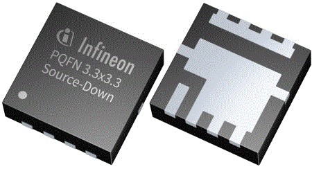
2022-01-07 | ReturnCompared to the standard Drain-Down concept, the latest Source-Down package technology enables a larger silicon die in the same package outline. In addition, the losses contributed by the package, limiting the overall performance of the device, can be reduced. This enables a reduction in R DS(on) by up to 30 percent compared to the state of the art Drain-Down package. The benefit at the system level is a shrink in the form factor with the possibility to move from a SuperSO8 5 x 6 mm 2 footprint to a PQFN 3.3 x 3.3 mm 2 package with a space reduction of about 65 percent. This allows for the available space to be used more effectively, enhancing the power density and system efficiency in the end system.
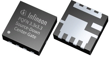
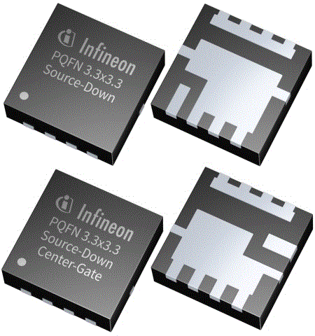
Additionally, in the Source-Down concept, the heat is dissipated directly into the PCB through a thermal pad instead of over the bond wire or the copper clip. This improves the thermal resistance R thJC by more than 20 percent, from 1.8 K/W down to 1.4 K/W, thus enabling simplified thermal management. Infineon offers two different footprint versions and layout options: the SD Standard-Gate and the SD Center-Gate. The Standard-Gate layout simplifies the drop-in replacement of Drain-Down packages, while the Center-Gate layout enables optimized and easier parallelization. These two options can bring optimal device arrangement in the PCB, optimized PCB parasitics, and ease of use.
Availability
OptiMOS™ Source-Down power MOSFETs are now available in PQFN 3.3 x 3.3 mm 2 packaging, a wide range of voltage classes from 25 up to 100 V, and two different footprint versions. More information is available at www.infineon.com/source-down.
More information about Infineon’s contribution to energy efficiency: www.infineon.com/green-energy
Information Number
INFPSS202201-041
Press Photos
The new generation of OptiMOS™ Source-Down (SD) power MOSFETs from Infineon come in a PQFN 3.3 x 3.3 mm2 package and a wide voltage class ranging from 25 V up to 100 V. The package enables a reduction in RDS(on) by up to 30 percent compared to the state of the art Drain-Down package. Additionally, the heat is dissipated directly into the PCB through a thermal pad instead of over the bond wire or the copper clip. This improves the thermal resistance RthJC by more than 20 percent, from 1.8 K/W down to 1.4 K/W.
PQFN_SD_CG

PQFN_SD_combi

PQFN_SDplusCG

Source: https://www.infineon.com


