Manufacturers
- Abracon
- Adam Tech
- Aerospace, Defense & Marine
- Agastat
- AIC
- AKM Semiconductor
- Alcoswitch
- Allegro
- Alps Electric
- Altera
- AMI Semiconductor
- AMP
- ams
- Analog Devices (ADI)
- Aptina Imaging
- Atmel
- Avago / Broadcom
- AVX
- Axicom
- Bccomponents
- Beyschlag
- BI Technologies
- Bourns Inc.
- Bowei Integrated Circuits
- Bridgelux
- Buchanan
- California Micro Devices
- Catalyst Semiconductor
- CGS
- Cirrus Logic
- Citizen Electronics
- CML Microcircuits
- Coiltronics
- Cooper Bussmann
- Corcom
- Core Logic
- Cree
- CSR PLC
- CTS
- Cypress Semiconductor
- Dale
- Data Image
- Deutsch
- Diodes Incorporated
- DOMINANT Opto Technologies
- E-T-A
- Eaton
- ECS
- Edison Opto
- Elcon
- EPCOS
- Epistar
- Epson
- Everlight Electronics
- Exar
- Fairchild Semiconductor
- FCI
- Freescale Semiconductor
- Fremont Micro Devices (FMD)
- Fujitsu Semiconductor
- Fulltech Electric
- General Semiconductor
- Harvatek
- Holsworthy
- Hsuan Mao Technology
- IDT
- Infineon Technologies
- Innolux
- International Rectifier (IR)
- Intersil
- IRC
- ISSI
- IXYS-IC
- Jing Cheng Electronical
- JL World
- Johanson Dielectrics
- Johanson Technology
- JRC / NJR
- JST
- KEC
- Kilovac
- Kingbright
- Kyocera Industrial Ceramics
- LEDiL
- Linear Technology / ADI
- Lite-On Technology
- Littelfuse
- Lumex
- Lumileds
- Luminary Micro
- Luminus Devices
- Macronix
- Maojwei / ZJPT
- Maxim Integrated
- MCC
- Mean Well Enterprises
- Microchip Technology
- Micron
- Microsemi
- Mini-Circuits
- Molex
- Murata Manufacturing
- Murata Power Solutions
- MWT
- National Semiconductor
- Nichicon
- Nippon Chemi-Con
- NJR / JRC
- NVE
- NXP Semiconductors
- OEG
- Omnivision
- ON Semiconductor
- Optek Technology
- Optrex
- OSRAM Opto Semiconductors
- OTAX
- Panasonic
- Peregrine(pSemi)
- Potter & Brumfield
- Power Integrations
- PowerStor
- Preci-Dip
- Prewell
- Products Unlimited
- Pulse Electronics
- PulseCore Semiconductor
- Qorvo
- Raychem
- Renesas Electronics
- RFMD
- Richtek Technology
- ROHM Semiconductor
- Rubycon
- Samsung Electro-Mechanics
- Samsung Semiconductor
- Schaffner
- Schrack
- Seiko Instruments, Inc. (SII)
- Semtech
- Sensata
- Seoul Semiconductor
- Sfernice
- Sharp Display
- Sharp Microelectronics
- Silicon Labs
- Siliconix
- Skyworks Solutions
- SoniCrest / JL World
- Spansion
- Sprague
- Stanley Electric
- STMicroelectronics
- Sunny Electronics
- Susumu (SSM)
- Taimag
- Taiyo Yuden
- TDK
- TDK-Lambda
- TE Connectivity
- Teccor
- Texas Instruments (TI)
- Thin Film
- Tianma Micro-electronics
- TOCOS
- TOKO
- Toshiba Electronic Components
- TT Electronics
- Tusonix
- TXC
- Tyntek
- Vishay
- Vishay Precision Group
- Vitramon
- Walsin Technology
- Weidmuller
- Welwyn
- Wickmann
- Winbond
- Xilinx
- Yageo
- Zetex Semiconductors
- ZJPT / Maojwei
News
Toshiba Starts Test-Sample Shipments of a Bare Die 1200V SiC MOSFET with Low On-Resistance and High Reliability, for Use in Automotive Traction Inverters
2025-01-15 | Return KAWASAKI, Japan—Toshiba Electronic Devices & Storage Corporation has developed "X5M007E120," a bare die[1] 1200V silicon carbide (SiC) MOSFET for automotive traction inverters[2] with an innovative structure that deliver both low On-resistance and high reliability. Test samples are now shipping, for evaluation by customers.
The reliability of typical SiC MOSFETs is degraded by increased On-resistance when its body diodes are bipolar energized[3] during reverse conduction operation[4]. Toshiba SiC MOSFETs alleviate this issue by a device structure that embeds Schottky barrier diodes (SBDs) into the MOSFET to inactivate body diodes, but positioning the SBDs on the chip reduces the area available for channels that determines the resistance of MOSFET On-operation and increases the chip’s On-resistance.
The SBDs embedded in X5M007E120 are arrayed in a check pattern, not the typically used striped pattern, an arrangement that effectively suppresses bipolar energization of the device’s body diodes, while improving the upper limit of unipolar operation to approximately twice the current area, even when taking up the same SBDs mounting area[5]. Channel density is also improved against the striped array, and On-resistance per unit area is low, reduced by approximately 20% to 30%[5]. This improved performance, low On-resistance while maintaining reliability against reverse conduction operation, will save energy in inverters used for motor control, such as automotive traction inverters.
Reducing On-resistance in an SiC MOSFET causes excess current flow through the MOSFET during short-circuit[6], reducing short-circuit durability. Enhancing the conduction of the embedded SBDs to improve the reliability of reverse conduction operation also increases current leakage during short-circuit, again decreasing short-circuit durability. The new bare die has a deep barrier structure[7] that suppresses excessive current in the MOSFET and leakage current in SBDs during short circuit status, improving its durability while maintaining excellent reliability against reverse conduction operation.
Users can customize the bare die to meet their specific design needs and realize solutions for their applications.
Toshiba expects to provide engineering samples of X5M007E120 in 2025, and to start mass production in 2026. In the meantime, it will explore further improvement to device characteristics.
Toshiba will contribute to the realization of a decarbonized society by providing customers with easier to use, higher performance power semiconductors for fields where energy efficiency is essential, such as inverters for motor control and power control systems for electric vehicles.
Notes:
[1] Unpackaged chip product.
[2] Equipment that converts battery-powered DC power to AC power and controls the motors in the electric vehicle (EV) or the hybrid vehicle (HEV).
[3] Bipolar operation when a forward voltage is applied to a pn diode between drain and source.
[4] An operation in which current flows from the source to the drain of the MOSFET due to the reflux of current in the circuit.
[5] Compared to Toshiba’s product using striped pattern.
[6] A phenomenon where long-term conduction occurs during abnormal mode such as control circuit failures, compared to short-term conduction during normal switching operation. Ruggedness that does not fail with a certain duration of short-circuit operation is required.
[7] An element of the device structure provided to control the high electric field due to high voltage. It greatly affects the performance of the device.
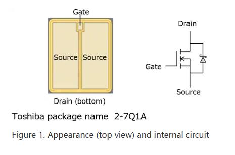
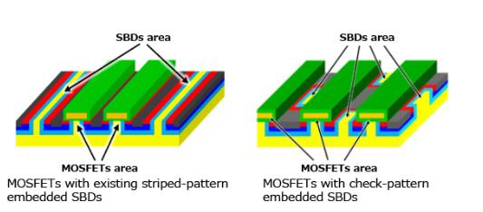
Figure 2. Schematic diagrams of MOSFETs with existing striped-pattern embedded SBDs and MOSFETs with check-pattern embedded SBDs
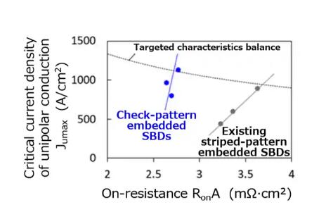
Figure 3. Measured values of critical current density of unipolar conduction and On-resistance of MOSFETs with existing striped-pattern embedded SBDs and MOSFETs with check-pattern embedded SBDs (Toshiba survey)
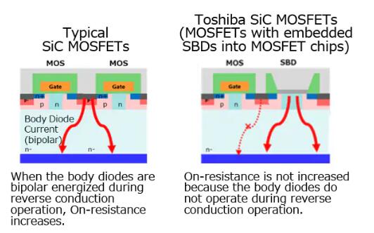
Figure 4. Comparison between typical SiC MOSFETs and Toshiba SiC MOSFETs (MOSFETs with embedded SBDs into MOSFET chips)
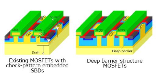
Figure 5. Schematic diagrams of existing MOSFETs with check-pattern embedded SBDs and deep barrier structure MOSFETs
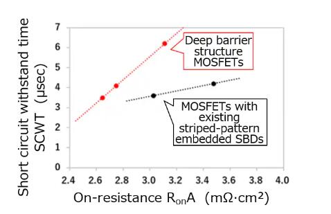
Figure 6. Measured values of short circuit withstand times and On-resistance of MOSFETs with existing striped-pattern embedded SBDs and deep barrier structure MOSFETs (Toshiba survey)
Applications
Automotive traction inverters
Features
Low On-resistance and high reliability
Bare die for automotive
AEC-Q100 qualified
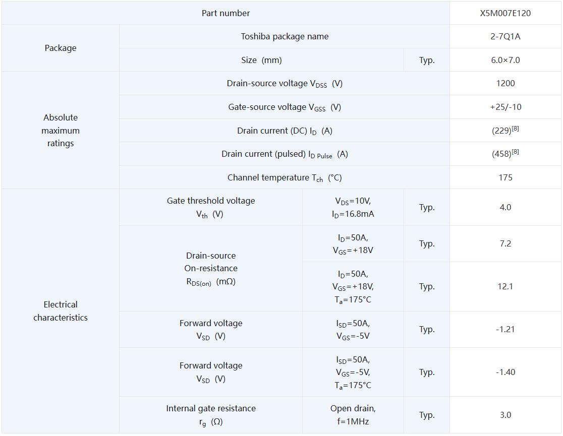
Drain-source voltage rating: VDSS=1200V
Drain current (DC) rating: ID=(229)A[8]
Low On-resistance:
RDS(ON)=7.2mΩ (typ.) (VGS=+18V, Ta=25°C)
RDS(ON)=12.1mΩ (typ.) (VGS=+18V, Ta=175°C)
Note
[8] Tentative values
Main Specifications
(Ta=25°C, unless otherwise specified)
Follow the link below for more on Toshiba’s SiC Power Devices.
SiC Power Devices
Source:https://toshiba.semicon-storage.com/


