Manufacturers
- Abracon
- Adam Tech
- Aerospace, Defense & Marine
- Agastat
- AIC
- AKM Semiconductor
- Alcoswitch
- Allegro
- Alps Electric
- Altera
- AMI Semiconductor
- AMP
- ams
- Analog Devices (ADI)
- Aptina Imaging
- Atmel
- Avago / Broadcom
- AVX
- Axicom
- Bccomponents
- Beyschlag
- BI Technologies
- Bourns Inc.
- Bowei Integrated Circuits
- Bridgelux
- Buchanan
- California Micro Devices
- Catalyst Semiconductor
- CGS
- Cirrus Logic
- Citizen Electronics
- CML Microcircuits
- Coiltronics
- Cooper Bussmann
- Corcom
- Core Logic
- Cree
- CSR PLC
- CTS
- Cypress Semiconductor
- Dale
- Data Image
- Deutsch
- Diodes Incorporated
- DOMINANT Opto Technologies
- E-T-A
- Eaton
- ECS
- Edison Opto
- Elcon
- EPCOS
- Epistar
- Epson
- Everlight Electronics
- Exar
- Fairchild Semiconductor
- FCI
- Freescale Semiconductor
- Fremont Micro Devices (FMD)
- Fujitsu Semiconductor
- Fulltech Electric
- General Semiconductor
- Harvatek
- Holsworthy
- Hsuan Mao Technology
- IDT
- Infineon Technologies
- Innolux
- International Rectifier (IR)
- Intersil
- IRC
- ISSI
- IXYS-IC
- Jing Cheng Electronical
- JL World
- Johanson Dielectrics
- Johanson Technology
- JRC / NJR
- JST
- KEC
- Kilovac
- Kingbright
- Kyocera Industrial Ceramics
- LEDiL
- Linear Technology / ADI
- Lite-On Technology
- Littelfuse
- Lumex
- Lumileds
- Luminary Micro
- Luminus Devices
- Macronix
- Maojwei / ZJPT
- Maxim Integrated
- MCC
- Mean Well Enterprises
- Microchip Technology
- Micron
- Microsemi
- Mini-Circuits
- Molex
- Murata Manufacturing
- Murata Power Solutions
- MWT
- National Semiconductor
- Nichicon
- Nippon Chemi-Con
- NJR / JRC
- NVE
- NXP Semiconductors
- OEG
- Omnivision
- ON Semiconductor
- Optek Technology
- Optrex
- OSRAM Opto Semiconductors
- OTAX
- Panasonic
- Peregrine(pSemi)
- Potter & Brumfield
- Power Integrations
- PowerStor
- Preci-Dip
- Prewell
- Products Unlimited
- Pulse Electronics
- PulseCore Semiconductor
- Qorvo
- Raychem
- Renesas Electronics
- RFMD
- Richtek Technology
- ROHM Semiconductor
- Rubycon
- Samsung Electro-Mechanics
- Samsung Semiconductor
- Schaffner
- Schrack
- Seiko Instruments, Inc. (SII)
- Semtech
- Sensata
- Seoul Semiconductor
- Sfernice
- Sharp Display
- Sharp Microelectronics
- Silicon Labs
- Siliconix
- Skyworks Solutions
- SoniCrest / JL World
- Spansion
- Sprague
- Stanley Electric
- STMicroelectronics
- Sunny Electronics
- Susumu (SSM)
- Taimag
- Taiyo Yuden
- TDK
- TDK-Lambda
- TE Connectivity
- Teccor
- Texas Instruments (TI)
- Thin Film
- Tianma Micro-electronics
- TOCOS
- TOKO
- Toshiba Electronic Components
- TT Electronics
- Tusonix
- TXC
- Tyntek
- Vishay
- Vishay Precision Group
- Vitramon
- Walsin Technology
- Weidmuller
- Welwyn
- Wickmann
- Winbond
- Xilinx
- Yageo
- Zetex Semiconductors
- ZJPT / Maojwei
뉴스
Toshiba’s New SiC MOSFETs Delivers Low On-Resistance and Significantly Reduced Switching Loss
2022-07-22 | 반환Power devices are essential components for managing and reducing power consumption in all kinds of electronic equipment, and for achieving a carbon neutral society. SiC is widely seen as the next generation material for power devices, as it delivers higher voltages and lower losses than silicon. While SiC power devices are now mainly utilized in inverters for trains, wider application is on the horizon, in vehicle electrification and the miniaturization of industrial equipment. However, the adoption and market growth of SiC devices have been held back by reliability issues.
Toshiba has solved this problem by adopting a structure in which a Schottky Barrier Diode (SBD) is placed in parallel with the PN diode inside the SiC MOSFET of the second-generation product. However, this created a new problem, whereby the performance of the MOSFET deteriorates when it includes an SBD cell that does not operate as a MOSFET. Specifically, there is an increase in the on-resistance per unit area (RonA) and in the performance index that indicates the on-resistance and high speed (Ron*Qgd). A further problem was a higher unit cost from increasing the chip area to reduce on-resistance (Ron).
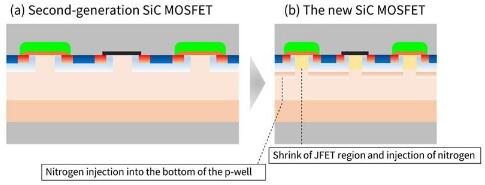
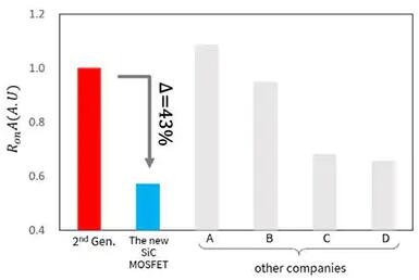
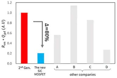
Toshiba has now developed a device structure that reduces RonA while including an SBD. Spread resistance (Rspread)[2] is reduced and the SBD current is increased by injecting nitrogen into the bottom of the wide p-type diffusion region (p-well) of the SiC MOSFET. Toshiba also reduced the JFET[3] region and injected nitrogen to reduce feedback capacitance and JFET resistance. As a result, feedback capacitance was reduced without increasing RonA. Toshiba prototyped and confirmed that this device structure reduces RonA by 43%[4], Ron*Qgd by 80%[5], and switching loss (from switching on and off) by about 20%[6], compared to its second-generation products. Stable operation without fluctuation of RonA was also secured by optimized positioning of the SBD.
Details of the achievement were reported at the PCIM Europe 2022, an international conference of power devices held in Nuremberg, Germany and online on May 12. Toshiba plans to start mass production of third generation SiC MOSFETs with the new technology in late August this year.
[1] MOSFET: metal-oxide-semiconductor field-effect transistor
[2] Spread resistance: The diffusion resistance at the bottom of the p-well.
[3] JFET: Junction Field Effect Transistor
[4] Comparison of the new 1.2kV SiC MOSFET when RonA is set to 1 in the second-generation SiC MOSFET. (Toshiba test results)
[5] Comparison of the new 1.2kV SiC MOSFET when Ron*Qgd is set to 1 in the second-generation SiC MOSFET. (Toshiba test results)
[6] Comparison of the new 1.2kV SiC MOSFET and the second-generation SiC MOSFET. (Toshiba test results)
The structure of Toshiba’s new SiC MOSFET

Reduction of RonA and Ron*Qgd (Toshiba test results)

(a) Comparison of RonA between the new 1.2kV SiC MOSFETs and the latest generation of SiC MOSFETs of other companies when RonA of its second-generation SiC MOSFETs is taken as 1.

(b) Comparison of Ron*Qgd between the new 1.2kV SiC MOSFETs and the latest generation of SiC MOSFETs of other companies when Ron*Qgd of its second-generation SiC MOSFETs is taken as 1.
Source: https://www.global.toshiba


