Manufacturers
- Abracon
- Adam Tech
- Aerospace, Defense & Marine
- Agastat
- AIC
- AKM Semiconductor
- Alcoswitch
- Allegro
- Alps Electric
- Altera
- AMI Semiconductor
- AMP
- ams
- Analog Devices (ADI)
- Aptina Imaging
- Atmel
- Avago / Broadcom
- AVX
- Axicom
- Bccomponents
- Beyschlag
- BI Technologies
- Bourns Inc.
- Bowei Integrated Circuits
- Bridgelux
- Buchanan
- California Micro Devices
- Catalyst Semiconductor
- CGS
- Cirrus Logic
- Citizen Electronics
- CML Microcircuits
- Coiltronics
- Cooper Bussmann
- Corcom
- Core Logic
- Cree
- CSR PLC
- CTS
- Cypress Semiconductor
- Dale
- Data Image
- Deutsch
- Diodes Incorporated
- DOMINANT Opto Technologies
- E-T-A
- Eaton
- ECS
- Edison Opto
- Elcon
- EPCOS
- Epistar
- Epson
- Everlight Electronics
- Exar
- Fairchild Semiconductor
- FCI
- Freescale Semiconductor
- Fremont Micro Devices (FMD)
- Fujitsu Semiconductor
- Fulltech Electric
- General Semiconductor
- Harvatek
- Holsworthy
- Hsuan Mao Technology
- IDT
- Infineon Technologies
- Innolux
- International Rectifier (IR)
- Intersil
- IRC
- ISSI
- IXYS-IC
- Jing Cheng Electronical
- JL World
- Johanson Dielectrics
- Johanson Technology
- JRC / NJR
- JST
- KEC
- Kilovac
- Kingbright
- Kyocera Industrial Ceramics
- LEDiL
- Linear Technology / ADI
- Lite-On Technology
- Littelfuse
- Lumex
- Lumileds
- Luminary Micro
- Luminus Devices
- Macronix
- Maojwei / ZJPT
- Maxim Integrated
- MCC
- Mean Well Enterprises
- Microchip Technology
- Micron
- Microsemi
- Mini-Circuits
- Molex
- Murata Manufacturing
- Murata Power Solutions
- MWT
- National Semiconductor
- Nichicon
- Nippon Chemi-Con
- NJR / JRC
- NVE
- NXP Semiconductors
- OEG
- Omnivision
- ON Semiconductor
- Optek Technology
- Optrex
- OSRAM Opto Semiconductors
- OTAX
- Panasonic
- Peregrine(pSemi)
- Potter & Brumfield
- Power Integrations
- PowerStor
- Preci-Dip
- Prewell
- Products Unlimited
- Pulse Electronics
- PulseCore Semiconductor
- Qorvo
- Raychem
- Renesas Electronics
- RFMD
- Richtek Technology
- ROHM Semiconductor
- Rubycon
- Samsung Electro-Mechanics
- Samsung Semiconductor
- Schaffner
- Schrack
- Seiko Instruments, Inc. (SII)
- Semtech
- Sensata
- Seoul Semiconductor
- Sfernice
- Sharp Display
- Sharp Microelectronics
- Silicon Labs
- Siliconix
- Skyworks Solutions
- SoniCrest / JL World
- Spansion
- Sprague
- Stanley Electric
- STMicroelectronics
- Sunny Electronics
- Susumu (SSM)
- Taimag
- Taiyo Yuden
- TDK
- TDK-Lambda
- TE Connectivity
- Teccor
- Texas Instruments (TI)
- Thin Film
- Tianma Micro-electronics
- TOCOS
- TOKO
- Toshiba Electronic Components
- TT Electronics
- Tusonix
- TXC
- Tyntek
- Vishay
- Vishay Precision Group
- Vitramon
- Walsin Technology
- Weidmuller
- Welwyn
- Wickmann
- Winbond
- Xilinx
- Yageo
- Zetex Semiconductors
- ZJPT / Maojwei
뉴스
Infineon adds PQFN Dual-Side Cooling 25-150 V portfolio to its OptiMOS™ Source-Down power MOSFET family
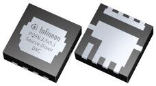
2022-12-15 | 반환The new portfolio combines Infineon’s latest MOSFET technology with leading-edge packaging to bring system performance to the next level. In the Source-Down (SD) concept, the MOSFET die source contact is flipped toward the footprint side of the package, which is then soldered to the PCB. In addition, the concept comprises an improved clip design on top of the chip for the drain contact and market-leading chip-to-package area ratio.
As system form factors continuously shrink, two key aspects are essential: reduction of power losses and optimal thermal management. Compared to best-in-class PQFN 3.3 x 3.3 m² Drain-Down devices, the new family significantly improves the on-resistance (R DS(on)) by up to 25 percent. Infineon’s OptiMOS Source-Down PQFN with Dual-Side Cooling provides an enhanced thermal interface to redirect power losses from the switch towards the heatsink. Dual-Side Cooling variants offer the most direct way to connect a power switch to a heatsink, increasing power dissipation capability by a factor of up to three compared to the corresponding Bottom-Side Cooled Source-Down variant.
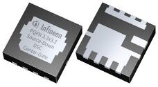
Two different footprint variants are available to offer the highest flexibility for PCB routing. A traditional Standard-Gate variant provides a quick and easy modification of existing Drain-Down designs. And a Center-Gate (CG) variant opens new possibilities for paralleling devices to keep the driver-to-gate connection as short as possible. With an outstanding continuous current capability of up to 298 A, the entire OptiMOS Source-Down PQFN 3.3 x 3.3 mm² 25-150 V product family enables the highest system performance.
Availability
The OptiMOS Source-Down PQFN 3.3 x 3.3 mm² 25-150 V product family includes two footprint versions, Standard- and Center-Gate. Both variants in the Dual-Side Cooling package can be ordered now. More information is available at www.infineon.com/source-down.
More information about Infineon’s contribution to energy efficiency: www.infineon.com/green-energy.
Press Photos


Infineon’s OptiMOS Source-Down PQFN 3.3 x 3.3 mm² 25-150 V product family includes two footprint versions, Standard- and Center-Gate. Compared to best-in-class PQFN 3.3 x 3.3 m² Drain-Down devices, the new family significantly improves the on-resistance (RDS(on)) by up to 25 percent. With a Dual-Side Cooling package it provides an enhanced thermal interface to redirect power losses from the switch towards the heatsink increasing power dissipation capability by a factor of up to three compared to the corresponding Bottom-Side Cooled Source-Down variant.
▶ OptiMOS_Source-Down_DSC_WHSON
▶ OptiMOS_Source-Down_DSC_WHTFN
Source: https://www.infineon.com


