 sales@aoelectronics.com
 +86 755 2821 9272


- Abracon
- Adam Tech
- Aerospace, Defense & Marine
- Agastat
- AIC
- AKM Semiconductor
- Alcoswitch
- Allegro
- Alps Electric
- Altera
- AMI Semiconductor
- AMP
- ams
- Analog Devices (ADI)
- Aptina Imaging
- Atmel
- Avago / Broadcom
- AVX
- Axicom
- Bccomponents
- Beyschlag
- BI Technologies
- Bourns Inc.
- Bowei Integrated Circuits
- Bridgelux
- Buchanan
- California Micro Devices
- Catalyst Semiconductor
- CGS
- Cirrus Logic
- Citizen Electronics
- CML Microcircuits
- Coiltronics
- Cooper Bussmann
- Corcom
- Core Logic
- Cree
- CSR PLC
- CTS
- Cypress Semiconductor
- Dale
- Data Image
- Deutsch
- Diodes Incorporated
- DOMINANT Opto Technologies
- E-T-A
- Eaton
- ECS
- Edison Opto
- Elcon
- EPCOS
- Epistar
- Epson
- Everlight Electronics
- Exar
- Fairchild Semiconductor
- FCI
- Freescale Semiconductor
- Fremont Micro Devices (FMD)
- Fujitsu Semiconductor
- Fulltech Electric
- General Semiconductor
- Harvatek
- Holsworthy
- Hsuan Mao Technology
- IDT
- Infineon Technologies
- Innolux
- International Rectifier (IR)
- Intersil
- IRC
- ISSI
- IXYS-IC
- Jing Cheng Electronical
- JL World
- Johanson Dielectrics
- Johanson Technology
- JRC / NJR
- JST
- KEC
- Kilovac
- Kingbright
- Kyocera Industrial Ceramics
- LEDiL
- Linear Technology / ADI
- Lite-On Technology
- Littelfuse
- Lumex
- Lumileds
- Luminary Micro
- Luminus Devices
- Macronix
- Maojwei / ZJPT
- Maxim Integrated
- MCC
- Mean Well Enterprises
- Microchip Technology
- Micron
- Microsemi
- Mini-Circuits
- Molex
- Murata Manufacturing
- Murata Power Solutions
- MWT
- National Semiconductor
- Nichicon
- Nippon Chemi-Con
- NJR / JRC
- NVE
- NXP Semiconductors
- OEG
- Omnivision
- ON Semiconductor
- Optek Technology
- Optrex
- OSRAM Opto Semiconductors
- OTAX
- Panasonic
- Peregrine(pSemi)
- Potter & Brumfield
- Power Integrations
- PowerStor
- Preci-Dip
- Prewell
- Products Unlimited
- Pulse Electronics
- PulseCore Semiconductor
- Qorvo
- Raychem
- Renesas Electronics
- RFMD
- Richtek Technology
- ROHM Semiconductor
- Rubycon
- Samsung Electro-Mechanics
- Samsung Semiconductor
- Schaffner
- Schrack
- Seiko Instruments, Inc. (SII)
- Semtech
- Sensata
- Seoul Semiconductor
- Sfernice
- Sharp Display
- Sharp Microelectronics
- Silicon Labs
- Siliconix
- Skyworks Solutions
- SoniCrest / JL World
- Spansion
- Sprague
- Stanley Electric
- STMicroelectronics
- Sunny Electronics
- Susumu (SSM)
- Taimag
- Taiyo Yuden
- TDK
- TDK-Lambda
- TE Connectivity
- Teccor
- Texas Instruments (TI)
- Thin Film
- Tianma Micro-electronics
- TOCOS
- TOKO
- Toshiba Electronic Components
- TT Electronics
- Tusonix
- TXC
- Tyntek
- Vishay
- Vishay Precision Group
- Vitramon
- Walsin Technology
- Weidmuller
- Welwyn
- Wickmann
- Winbond
- Xilinx
- Yageo
- Zetex Semiconductors
- ZJPT / Maojwei
News
A general-purpose package is newly available in the lineup of Toshiba’s small, surface mount LDO regulator which enables long operation and operational stability of IoT equipment : TCR3UF series
2020-02-27 | Return Toshiba Electronic Devices & Storage Corporation have developed 74 types of "TCR3UF series", small surface mount LDO regulators which adopt SMV package with a maximum output current of 300 mA. And they have extended Toshiba’s lineup.
The new "TCR3UF series" is for power management of IoT equipment, wearable devices, mobile devices, etc. It has low consumption current characteristics, and features an industry's leading trade-off between high ripple rejection ratio and high speed load transient response[1]. Various protection functions such as overheat protection, overcurrent protection, and inrush current limiter are also incorporated.
In addition to the previously released compact and low height WCSP4F package "TCR3UG series" and the small and general-purpose DFN4 package "TCR3UM series", the new lead type and general-purpose SMV package "TCR3UF series" has been released this time.
The TCR3UF series is suitable for battery-powered devices that operate for a long time and power supplies for sensors that are susceptible to voltage fluctuations such as noise. There are 37 types of output voltage in the range of 0.8 V to 5.0 V, and a total of 74 types are available, with or without auto-discharge. Products can be selected according to the intended application.
Notes :
[1] By an output current 300 mA LDO regulator, as of January 2020, from a survey by Toshiba.
Features
General-purpose SMV packages : 2.9×2.8 mm (typ.), t=1.1 mm (typ.)
Low consumption current (Low quiescent current) : IB(ON1)=0.34 μA (typ.)
High ripple rejection ratio, high speed road transient response : R.R.=70 dB (typ.), ⊿VOUT= -51/+36 mV (typ.)
Applications
IoT equipment
Wearable devices (Hearable devices, etc.)
Mobile devices, etc.
Product Specifications
Part number |
TCR3UF series |
|||
Packages |
Name |
DFN4 |
WCSP4F |
SMV |
Size typ. (mm) |
1.0×1.0, |
0.645×0.645, |
2.9×2.8, |
|
Operating ranges |
Output current IOUT max (mA) |
300 |
||
Output voltage VOUT (V) |
0.8 to 5.0 |
|||
Input voltage VIN (V) |
1.5 to 5.5 |
|||
Operating temperature Topr (°C) |
-40 to 85 |
|||
Electrical |
Quiescent current IB(ON1) typ. (μA) |
0.34 |
||
Stand-by current IB(OFF1) typ. (μA) |
0.03 |
|||
Ripple rejection ratio R.R. typ. (dB) |
70 |
|||
Drop-out voltage VDO typ. (mV) |
196 |
140 |
206 |
|
Load transient response ⊿VOUT typ. (mV) |
-51/+36 |
-60/+60 |
-51/+36 |
|
Notes :
[2] Common test conditions : Unless otherwise specified, @VIN=VOUT+1 V (VOUT>1.5 V), VIN=2.5 V (VOUT≤1.5 V),
IOUT=50 mA, CIN=1.0 μF, COUT=1.0 μF
[3] New products
Block Diagram
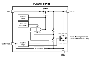
Note : Some of the functional blocks, circuits, or constants in the block diagram may be omitted or simplified for explanatory purposes.
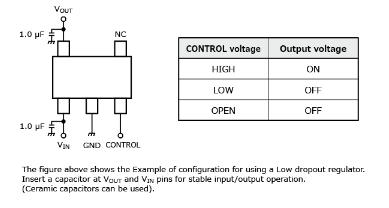
Example of Application Circuit
Source: http://www.semicon.toshiba.co.jp/eng/