 sales@aoelectronics.com
 +86 755 2821 9272


Manufacturers
- Abracon
- Adam Tech
- Aerospace, Defense & Marine
- Agastat
- AIC
- AKM Semiconductor
- Alcoswitch
- Allegro
- Alps Electric
- Altera
- AMI Semiconductor
- AMP
- ams
- Analog Devices (ADI)
- Aptina Imaging
- Atmel
- Avago / Broadcom
- AVX
- Axicom
- Bccomponents
- Beyschlag
- BI Technologies
- Bourns Inc.
- Bowei Integrated Circuits
- Bridgelux
- Buchanan
- California Micro Devices
- Catalyst Semiconductor
- CGS
- Cirrus Logic
- Citizen Electronics
- CML Microcircuits
- Coiltronics
- Cooper Bussmann
- Corcom
- Core Logic
- Cree
- CSR PLC
- CTS
- Cypress Semiconductor
- Dale
- Data Image
- Deutsch
- Diodes Incorporated
- DOMINANT Opto Technologies
- E-T-A
- Eaton
- ECS
- Edison Opto
- Elcon
- EPCOS
- Epistar
- Epson
- Everlight Electronics
- Exar
- Fairchild Semiconductor
- FCI
- Freescale Semiconductor
- Fremont Micro Devices (FMD)
- Fujitsu Semiconductor
- Fulltech Electric
- General Semiconductor
- Harvatek
- Holsworthy
- Hsuan Mao Technology
- IDT
- Infineon Technologies
- Innolux
- International Rectifier (IR)
- Intersil
- IRC
- ISSI
- IXYS-IC
- Jing Cheng Electronical
- JL World
- Johanson Dielectrics
- Johanson Technology
- JRC / NJR
- JST
- KEC
- Kilovac
- Kingbright
- Kyocera Industrial Ceramics
- LEDiL
- Linear Technology / ADI
- Lite-On Technology
- Littelfuse
- Lumex
- Lumileds
- Luminary Micro
- Luminus Devices
- Macronix
- Maojwei / ZJPT
- Maxim Integrated
- MCC
- Mean Well Enterprises
- Microchip Technology
- Micron
- Microsemi
- Mini-Circuits
- Molex
- Murata Manufacturing
- Murata Power Solutions
- MWT
- National Semiconductor
- Nichicon
- Nippon Chemi-Con
- NJR / JRC
- NVE
- NXP Semiconductors
- OEG
- Omnivision
- ON Semiconductor
- Optek Technology
- Optrex
- OSRAM Opto Semiconductors
- OTAX
- Panasonic
- Peregrine(pSemi)
- Potter & Brumfield
- Power Integrations
- PowerStor
- Preci-Dip
- Prewell
- Products Unlimited
- Pulse Electronics
- PulseCore Semiconductor
- Qorvo
- Raychem
- Renesas Electronics
- RFMD
- Richtek Technology
- ROHM Semiconductor
- Rubycon
- Samsung Electro-Mechanics
- Samsung Semiconductor
- Schaffner
- Schrack
- Seiko Instruments, Inc. (SII)
- Semtech
- Sensata
- Seoul Semiconductor
- Sfernice
- Sharp Display
- Sharp Microelectronics
- Silicon Labs
- Siliconix
- Skyworks Solutions
- SoniCrest / JL World
- Spansion
- Sprague
- Stanley Electric
- STMicroelectronics
- Sunny Electronics
- Susumu (SSM)
- Taimag
- Taiyo Yuden
- TDK
- TDK-Lambda
- TE Connectivity
- Teccor
- Texas Instruments (TI)
- Thin Film
- Tianma Micro-electronics
- TOCOS
- TOKO
- Toshiba Electronic Components
- TT Electronics
- Tusonix
- TXC
- Tyntek
- Vishay
- Vishay Precision Group
- Vitramon
- Walsin Technology
- Weidmuller
- Welwyn
- Wickmann
- Winbond
- Xilinx
- Yageo
- Zetex Semiconductors
- ZJPT / Maojwei
News
Toshiba Electronic Devices & Storage Corporation Introduces SOI Process with Low Noise Figure for Low-Noise RF Amplifiers for Smartphones
2018-01-26 | ReturnIn recent years, the increasing speed of mobile data communication has expanded use of RF switches and filters in the analog front end of mobile devices. The resulting increase in signal loss between antenna and receiver circuit has degraded receiver sensitivity, and focused attention on LNAs with a low noise figure[2] (NF) as a means to compensate for signal loss and improve the integrity of the received signal.
Toshiba Electronic Devices & Storage has used its new TaRF10 process to develop a prototype LNA with an outstanding noise figure of 0.72dB and a gain[3] of 16.9dB at a frequency of 1.8GHz.
Mobile devices use many RF switches and LNAs in the receiver circuit, generating a need to reduce circuit size in order to reduce board area utilization. Current LNAs typically use silicon-germanium-carbon (SiGe:C) bipolar transistors, and it has been difficult to integrate LNAs and RF switches fabricated with different processes on the same chip.
The new TaRF10 process can integrate LNAs, control circuits and RF switches on a single chip, as it is highly compatible with the TaRF8 and TaRF9 processes for RF switches, which secure outstanding RF characteristics. TaRF9 realizes lower insertion loss and signal distortion than TaRF8. Toshiba Electronic Devices & Storage now plans to bring to market LNAs with integrated RF switches.
Toshiba Electronic Devices & Storage has developed RF ICs utilizing its subsidiary, Japan Semiconductor Corporation to apply the latest SOI-CMOS technology, and by handling all aspects of the production flow, from RF process technology development to the design and manufacturing, secured a rapid products launch.
To meet next-generation market requirements for 5G smartphones, the company will continue to further improve the characteristics of the TarfSOI™ process and develop RF ICs with cutting-edge technology.
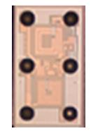
Fig.1. Appearance of LNA fabricated with TaRF10
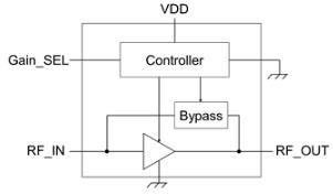
Fig.2. Functional block diagram of LNA
Table 1. Main Specifications of LNA
Mode |
LNA applying TaRF 10 process |
Unit |
|
Chip Size |
- |
0.70×0.43 |
Mm |
Frequency |
- |
1.8 |
GHz |
Supply Voltage |
- |
1.8 |
V |
Supply Current |
Gain mode |
7.4 |
mA |
Bypass mode |
50 |
μA |
|
Control Voltage |
Gain mode |
1.8 |
V |
Bypass mode |
0 |
V |
|
Gain |
Gain mode |
16.9 |
dB |
Bypass mode |
-1.6 |
dB |
|
NF |
Gain mode |
0.72 |
dB |
Return Loss (In) |
Gain mode |
8.4 |
dB |
Return Loss (Out) |
Gain mode |
12.1 |
dB |
Reverse Isolation |
Gain mode |
26.5 |
dB |
IP1dB |
Gain mode |
-8.9 |
dBm |
IIP3 |
Gain mode |
4.3 |
dBm |
Notes:
[1] TarfSOI™ (Toshiba advanced RF SOI): Toshiba’s unique SOI-CMOS (silicon-on-insulator-complementary metal oxide semiconductor) front-end process
[2] Noise figure: the ratio of signal-to-noise ratio at the output to that at the input. The lower the noise figure, the lower the amplifier self-noise is and therefore the better.
[3] Gain: the ratio of the output power of an amplifier to its input power in dB
Source:http://www.semicon.toshiba.co.jp/eng/