 sales@aoelectronics.com
 +86 755 2821 9272


Manufacturers
- Abracon
- Adam Tech
- Aerospace, Defense & Marine
- Agastat
- AIC
- AKM Semiconductor
- Alcoswitch
- Allegro
- Alps Electric
- Altera
- AMI Semiconductor
- AMP
- ams
- Analog Devices (ADI)
- Aptina Imaging
- Atmel
- Avago / Broadcom
- AVX
- Axicom
- Bccomponents
- Beyschlag
- BI Technologies
- Bourns Inc.
- Bowei Integrated Circuits
- Bridgelux
- Buchanan
- California Micro Devices
- Catalyst Semiconductor
- CGS
- Cirrus Logic
- Citizen Electronics
- CML Microcircuits
- Coiltronics
- Cooper Bussmann
- Corcom
- Core Logic
- Cree
- CSR PLC
- CTS
- Cypress Semiconductor
- Dale
- Data Image
- Deutsch
- Diodes Incorporated
- DOMINANT Opto Technologies
- E-T-A
- Eaton
- ECS
- Edison Opto
- Elcon
- EPCOS
- Epistar
- Epson
- Everlight Electronics
- Exar
- Fairchild Semiconductor
- FCI
- Freescale Semiconductor
- Fremont Micro Devices (FMD)
- Fujitsu Semiconductor
- Fulltech Electric
- General Semiconductor
- Harvatek
- Holsworthy
- Hsuan Mao Technology
- IDT
- Infineon Technologies
- Innolux
- International Rectifier (IR)
- Intersil
- IRC
- ISSI
- IXYS-IC
- Jing Cheng Electronical
- JL World
- Johanson Dielectrics
- Johanson Technology
- JRC / NJR
- JST
- KEC
- Kilovac
- Kingbright
- Kyocera Industrial Ceramics
- LEDiL
- Linear Technology / ADI
- Lite-On Technology
- Littelfuse
- Lumex
- Lumileds
- Luminary Micro
- Luminus Devices
- Macronix
- Maojwei / ZJPT
- Maxim Integrated
- MCC
- Mean Well Enterprises
- Microchip Technology
- Micron
- Microsemi
- Mini-Circuits
- Molex
- Murata Manufacturing
- Murata Power Solutions
- MWT
- National Semiconductor
- Nichicon
- Nippon Chemi-Con
- NJR / JRC
- NVE
- NXP Semiconductors
- OEG
- Omnivision
- ON Semiconductor
- Optek Technology
- Optrex
- OSRAM Opto Semiconductors
- OTAX
- Panasonic
- Peregrine(pSemi)
- Potter & Brumfield
- Power Integrations
- PowerStor
- Preci-Dip
- Prewell
- Products Unlimited
- Pulse Electronics
- PulseCore Semiconductor
- Qorvo
- Raychem
- Renesas Electronics
- RFMD
- Richtek Technology
- ROHM Semiconductor
- Rubycon
- Samsung Electro-Mechanics
- Samsung Semiconductor
- Schaffner
- Schrack
- Seiko Instruments, Inc. (SII)
- Semtech
- Sensata
- Seoul Semiconductor
- Sfernice
- Sharp Display
- Sharp Microelectronics
- Silicon Labs
- Siliconix
- Skyworks Solutions
- SoniCrest / JL World
- Spansion
- Sprague
- Stanley Electric
- STMicroelectronics
- Sunny Electronics
- Susumu (SSM)
- Taimag
- Taiyo Yuden
- TDK
- TDK-Lambda
- TE Connectivity
- Teccor
- Texas Instruments (TI)
- Thin Film
- Tianma Micro-electronics
- TOCOS
- TOKO
- Toshiba Electronic Components
- TT Electronics
- Tusonix
- TXC
- Tyntek
- Vishay
- Vishay Precision Group
- Vitramon
- Walsin Technology
- Weidmuller
- Welwyn
- Wickmann
- Winbond
- Xilinx
- Yageo
- Zetex Semiconductors
- ZJPT / Maojwei
News
Toshiba Launches its 3rd Generation SiC MOSFETs that Contribute to the Higher Efficiency of Industrial Equipment
2022-08-30 | Return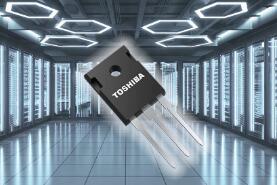
KAWASAKI, Japan— Toshiba Electronic Devices & Storage Corporation ("Toshiba") has launched new power devices, the “TWxxNxxxC series,” its 3rd generation silicon carbide(SiC) MOSFETs[1][2] that deliver low on-resistance and significantly reduced switching loss. Ten products, five 1200V and five 650V products, have started shipping today.
The new products reduce on-resistance per unit area (RDS(ON)A) by about 43%[3], allowing the drain-source on-resistance * gate-drain charge (RDS(ON)*Qgd), an important index that represents the relationship between conduction loss and switching loss, to be lowered by about 80%[4]. This cuts the switching loss by about 20%[5], and lowers both on-resistance and switching loss. The new products contribute to higher equipment efficiency.
Toshiba will continue to expand its lineup of power devices and to enhance its production facilities, and aims to realize a carbon-free economy by providing high-performance power devices that are easy to use.
Notes:
[1] Toshiba has developed a device structure that reduces on-resistance per unit area (RDS(ON)A) by using a structure with built-in schottky barrier diode developed for the 2nd generation MOSFETs, and also reduces feedback capacitance in the JFET region.
[2] MOSFET: metal-oxide-semiconductor field-effect transistor
[3] Comparison of the new 1200V SiC MOSFETs when RDS(ON)A is set to 1 in the 2nd generation SiC MOSFETs. Toshiba survey.
[4] Comparison of the new 1200V SiC MOSFETs when RDS(ON)*Qgd is set to 1 in the 2nd generation SiC MOSFETs. Toshiba survey.
[5] Comparison of the new 1200V SiC MOSFETs and the 2nd generation SiC MOSFETs. Toshiba survey.
Applications
● Switching power supplies (servers, data center, communications equipment, etc.)
● EV charging stations
● Photovoltaic inverters
● Uninterruptible power supplies (UPS)
Features
● Low on-resistance per unit area (RDS(ON)A)
● Low drain-source on-resistance * gate-drain charge (RDS(ON)*Qgd)
● Low diode forward voltage: VDSF = -1.35 V (typ.) @VGS = -5 V
Main Specifications
(@Ta=25°C unless otherwise specified)
Part number |
Package |
Absolute maximum ratings |
||||||||
Drain-source |
Gate-source |
Drain |
||||||||
@Tc=25℃ |
||||||||||
TO-247 |
1200 |
-10 to 25 |
100 |
|||||||
60 |
||||||||||
40 |
||||||||||
36 |
||||||||||
20 |
||||||||||
650 |
100 |
|||||||||
58 |
||||||||||
40 |
||||||||||
30 |
||||||||||
20 |
||||||||||
Electrical characteristics |
||||||||||
Drain- Source resistance |
Gate |
Total |
Gate- |
Input |
Diode |
|||||
@VGS=18V |
@VDS=10V |
@VDS=400V, |
@VGS= -5V |
|||||||
15 |
3.0 to 5.0 |
158 |
23 |
6000 |
-1.35 |
|||||
30 |
82 |
13 |
2925 |
|||||||
45 |
57 |
8.9 |
1969 |
|||||||
60 |
46 |
7.8 |
1530 |
|||||||
140 |
24 |
4.2 |
691 |
|||||||
15 |
128 |
19 |
4850 |
|||||||
27 |
65 |
10 |
2288 |
|||||||
48 |
41 |
6.2 |
1362 |
|||||||
83 |
28 |
3.9 |
873 |
|||||||
107 |
21 |
2.3 |
600 |
|||||||
Follow the links below for more on Toshiba SiC MOSFETs.
▶ SiC Power Devices
▶ SiC MOSFETs
Source: https://www.global.toshiba